
추천 제품


제품명
Monolayer graphene film, 1 cm x 1 cm on quartz, avg. no. of layers, 1
양식
film
특징
avg. no. of layers 1
저항성
600 Ω/sq
길이 × 너비 × 두께
1 cm × 1 cm × (theoretical) 0.345 nm, monolayer graphene film
1.25 cm × 1.25 cm × 525 μm, quartz substrate
유사한 제품을 찾으십니까? 방문 제품 비교 안내
일반 설명
Transfer Method: Clean transfer method
Quality Control: Optical Microscopy & Raman checked
Size: 1 cm x 1 cm
Appearance (Color): Transparent
Transparency: >97%
Appearance (Form): Film
Coverage: >95%
Number of graphene layers: 1
Thickness (theoretical): 0.345 nm
FET Electron Mobility on Al2O3: 2; 000 cm2/V·s
FET Electron Mobility on SiO2/Si (expected): 4; 000 cm2/V·s
Sheet Resistance: 600 Ohms/sq.
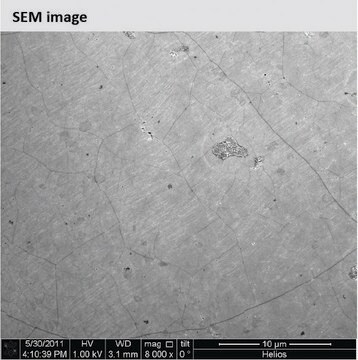
Grain size: Up to 10 μm
Substrate Quartz
Size: 1.25 cm x 1.25 cm
Flatness: bow: 20μm; warp: 30μm
Roughness:6 angstroms (on the polished side)
Surface: Double side polished
애플리케이션


신호어
Danger
유해 및 위험 성명서
Hazard Classifications
Carc. 1B - Eye Irrit. 2 - STOT RE 1 Inhalation - STOT SE 3
표적 기관
Lungs, Respiratory system
Storage Class Code
6.1D - Non-combustible acute toxic Cat.3 / toxic hazardous materials or hazardous materials causing chronic effects
WGK
WGK 3
Flash Point (°F)
Not applicable
Flash Point (°C)
Not applicable
문서
Professor Gogotsi and Dr. Shuck introduce MXenes: a promising family of two-dimensional materials with a unique combination of high conductivity, hydrophilicity, and extensive tunability.
Advanced technologies for energy conversion and storage are widely sought after for their potential to improve consumer and electronic device performance as well as for the prospect of reducing the societal and environmental impact of energy generation.
Graphene has emerged as the new wonder material. Being only one atom thick and composed of carbon atoms arranged in a hexagonal honeycomb lattice structure, the interest in this material has exploded exponentially since 2004 when it was first isolated and identified using a very simple method.
자사의 과학자팀은 생명 과학, 재료 과학, 화학 합성, 크로마토그래피, 분석 및 기타 많은 영역을 포함한 모든 과학 분야에 경험이 있습니다..
고객지원팀으로 연락바랍니다.