跳转至内容
Merck

560596

Sigma-Aldrich

PEDOT:PSS

low-conductivity grade, 2.7 wt. % aqueous dispersion

别名:

PEDOT:PSS, 聚(2,3-二氢噻吩并-1,4-二恶英)-聚(苯乙烯磺酸盐)

登录查看公司和协议定价


About This Item

MDL號碼:
分類程式碼代碼:
12352103
NACRES:
NA.23

product name

聚乙撑二氧噻吩-聚 苯乙烯磺酸盐, 2.7 wt % dispersion in H2O, low-conductivity grade

等級

low-conductivity grade

品質等級

成份

PEDOT content, ~0.14%
PSS content, ~2.6%

濃度

2.7 wt % dispersion in H2O

雜質

<300 ppm Na

粒徑

<200 nm, coeff var >95%

pH值

1.2-1.8

傅導性

~1E-5 S/cm

黏度

<20 cP(20 °C)

儲存溫度

2-8°C

正在寻找类似产品? 访问 产品对比指南

一般說明

最好采用旋涂法。建议使用前通过 0.45 μm 膜片过滤器过滤分散物。涂层在最高温度 200°C 下干燥 1 min,但温度在 50°C 至 150°C 之间通常就足够了。干燥层的最佳厚度在 50-250 nm 范围内。
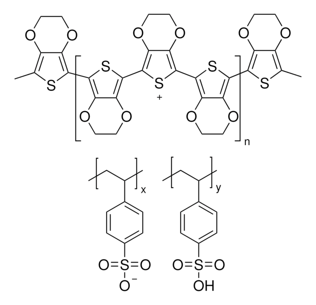
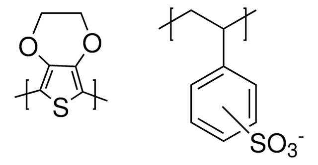
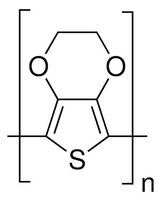
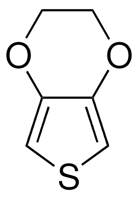
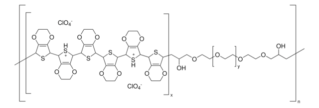
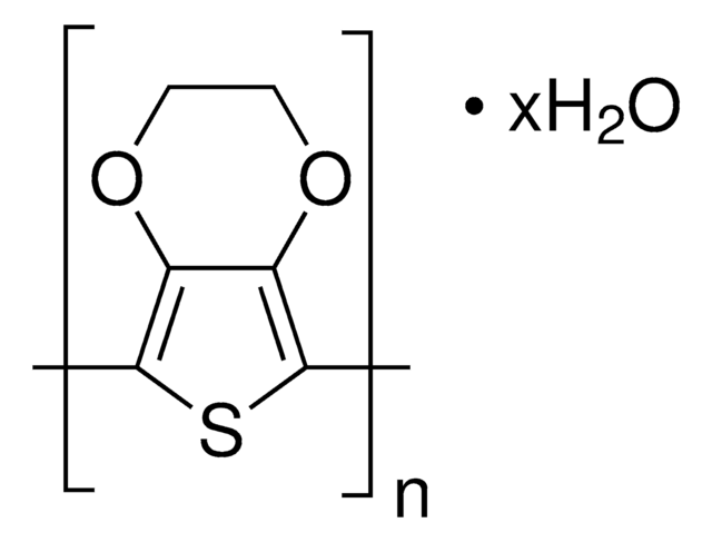
聚(3,4-乙撑二氧噻吩)-聚(苯乙烯磺酸盐)(PEDOT:PSS)是本征导电聚合物(ICP),由聚(3,4-乙撑二氧噻吩)(PEDOT)和聚(苯乙烯磺酸盐)(PSS)混合制得。它是水性乳液,其中PEDOT带正电,而PSS是反荷离子(带负电)。根据应用的不同,可以充当阳极或阴极材料。可用1000-5000 rpm的速度,将其旋涂在不同基底上。
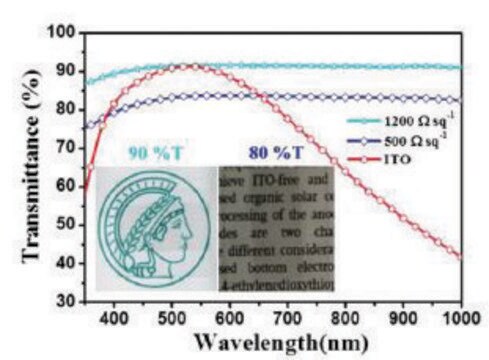
聚(苯乙烯磺酸)阴离子掺杂聚(3,4-乙烯二氧噻吩)等导电聚合物 (PEDOT/PSS) 广泛应用于各种有机光电器件中。PEDOT:PSS 是阳离子聚噻吩衍生物的混合物,掺杂有聚阴离子。这类聚合物的高导电性和良好的抗氧化性使其适用于电磁屏蔽和噪声抑制。因此,发现聚合物薄膜在整个可见光谱中具有高透明度,甚至进入近 IR 和近 UV 区域,在 900-2,000 nm 处几乎 100% 吸收。400-800 nm 处无最大吸收。已研究小电场和小磁场对聚合物的影响。

應用

PEDOT:PSS和聚(9-乙烯基咔唑)(PVK)可以交联形成多层有机发光二极管。质子交换膜(如Nafion 212)可用PEDOT:PSS和聚(烯丙胺盐酸盐)(PAH)逐层涂覆。
在 OLED 和 PLED 器件中用作界面空穴注入层,降低工作电压、提高发光效率、延长显示寿命。
从900nm到2000nm几乎100%吸收。从400nm到800nm无最大吸收。 导电聚合物混合。

特點和優勢

平均粒度更小,粒度分布更窄,可为 ITO 电极形成光滑表面,因此可降低 LED 设备短路的可能性。大幅降低的内在导电性可减少极小像素(小于 10 微米)矩阵阵列显示装置发生"串话"的可能性。

包裝

塑料瓶包装

象形圖

Corrosion

訊號詞

Danger

危險聲明

危險分類

Eye Dam. 1 - Skin Corr. 1

儲存類別代碼

8B - Non-combustible corrosive hazardous materials

水污染物質分類(WGK)

WGK 2

閃點(°F)

Not applicable

閃點(°C)

Not applicable

個人防護裝備

Faceshields, Gloves, Goggles, type ABEK (EN14387) respirator filter


从最新的版本中选择一种:

分析证书(COA)

Lot/Batch Number

没有发现合适的版本?

如果您需要特殊版本,可通过批号或批次号查找具体证书。

已有该产品?

在文件库中查找您最近购买产品的文档。

访问文档库

Opt. Mater., 9, 125-125 (1998)
Surface initiated oxidative crosslinking of a polymeric hole transport material for improved efficiency and lifetime in soluble organic light-emitting diodes
Jeon SK, et al.
Organic Electronics, 38(3) (2016)
Applied Physics Letters, 71, 34-34 (1997)
Synthetic Metals, 87, 171-171 (1997)
Conducting polymer electrodes for gel electrophoresis
Bengtsson K, et al.
PLoS ONE, 9(2), e89416-e89416 (2014)

商品

Tutorial Lithography Nanopatterning at Sigma-Aldrich. Lithography, based on traditional ink-printing techniques, is a process for patterning various layers, such as conductors, semiconductors, or dielectrics, on a surface.

In the emerging field of organic printable electronics, such as OLEDs and organic photovoltaics (OPVs), there is a significant need for improved organic conducting and semiconducting materials. This paper reports our recent progress in two fields: 1) the development of solvent-based dispersions of the intrinsically conducting polymer (ICP) poly(3,4- ethylenedioxythiophene) (PEDOT) and 2) the synthesis of new electron-deficient (n-type) semiconducting polymers.

Find advantages of inorganic interface layer inks for organic electronic & other applications.

Conducting polymers such as polyaniline, polythiophene and polyfluorenes are now much in the spotlight for their applications in organic electronics and optoelectronics.

查看所有结果

我们的科学家团队拥有各种研究领域经验,包括生命科学、材料科学、化学合成、色谱、分析及许多其他领域.

联系技术服务部门