
推荐产品
产品名称
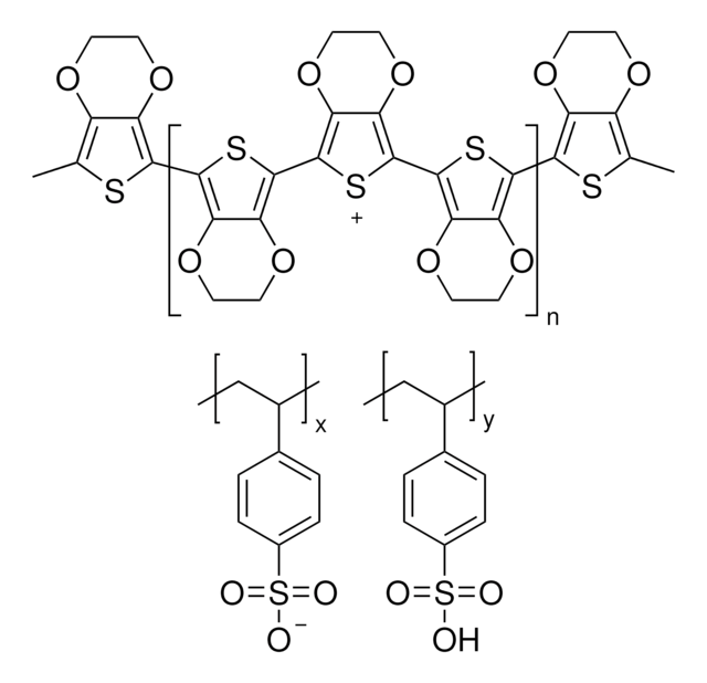
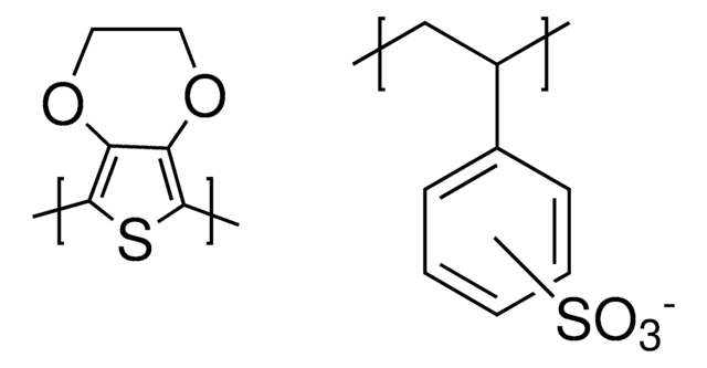
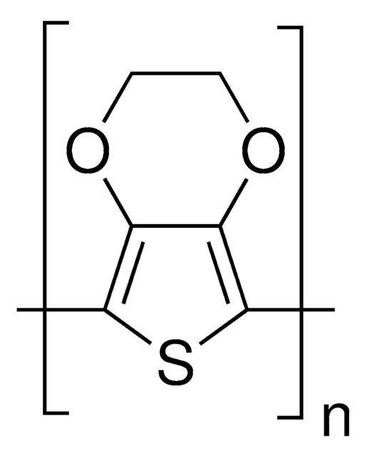
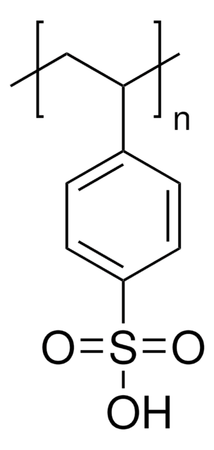
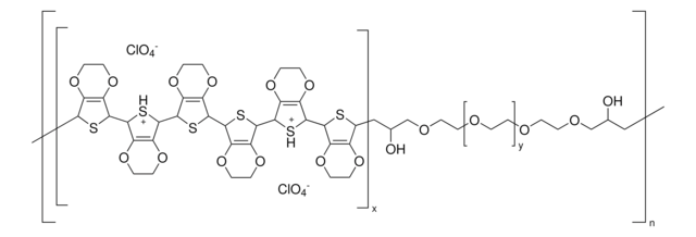
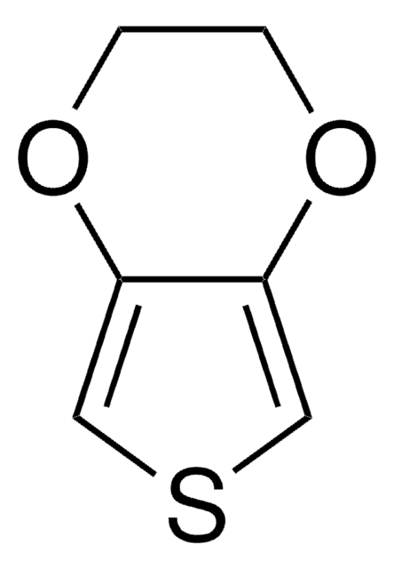
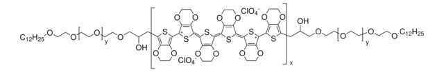
聚乙撑二氧噻吩-聚 苯乙烯磺酸盐, 1.3 wt % dispersion in H2O
成份
PEDOT content, 0.5 wt. %
PSS content, 0.8 wt. %
環保替代產品特色
Design for Energy Efficiency
Learn more about the Principles of Green Chemistry.
sustainability
Greener Alternative Product
濃度
1.3 wt % dispersion in H2O
帶隙
1.6 eV
傅導性
1 S/cm
環保替代類別
儲存溫度
2-8°C
正在寻找类似产品? 访问 产品对比指南
相关类别
一般說明
應用
特點和優勢
包裝

訊號詞
Danger
危險聲明
危險分類
Eye Dam. 1 - Skin Corr. 1
水污染物質分類(WGK)
WGK 2
個人防護裝備
Faceshields, Gloves, Goggles, type ABEK (EN14387) respirator filter
其他客户在看
商品
Tutorial Lithography Nanopatterning at Sigma-Aldrich. Lithography, based on traditional ink-printing techniques, is a process for patterning various layers, such as conductors, semiconductors, or dielectrics, on a surface.
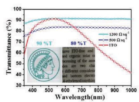
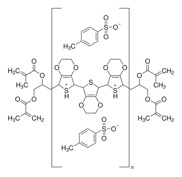
In the emerging field of organic printable electronics, such as OLEDs and organic photovoltaics (OPVs), there is a significant need for improved organic conducting and semiconducting materials. This paper reports our recent progress in two fields: 1) the development of solvent-based dispersions of the intrinsically conducting polymer (ICP) poly(3,4- ethylenedioxythiophene) (PEDOT) and 2) the synthesis of new electron-deficient (n-type) semiconducting polymers.
Find advantages of inorganic interface layer inks for organic electronic & other applications.
Conducting polymers such as polyaniline, polythiophene and polyfluorenes are now much in the spotlight for their applications in organic electronics and optoelectronics.
Global Trade Item Number
| 货号 | GTIN |
|---|---|
| 483095-250G | 4061838253880 |
我们的科学家团队拥有各种研究领域经验,包括生命科学、材料科学、化学合成、色谱、分析及许多其他领域.
联系客户支持