
773700
Graphene, monolayer film
1 cm x 1 cm on SiO2/Si substrate, avg. no. of layers, 1
Sinônimo(s):
Single Layer Graphene Sheet
About This Item
Produtos recomendados


Nome do produto
Monolayer graphene film, 1 cm x 1 cm on SiO2/Si substrate, avg. no. of layers, 1
Formulário
film
Características
avg. no. of layers 1
resistência
600 Ω/sq
C × L × espessura
1 cm × 1 cm × (theoretical) 0.345 nm, monolayer graphene film
1 cm × 1 cm × 525 μm, SiO2/Si substrate
Procurando produtos similares? Visita Guia de comparação de produtos
Categorias relacionadas
Descrição geral
Growth Method: CVD synthesis
Transfer Method: Clean transfer method
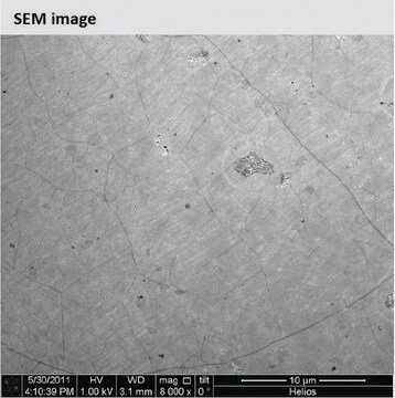
Quality Control: Optical Microscopy & Raman checked
Size: 1 cm x 1 cm
Appearance (Color): Transparent
Transparency: >97%
Appearance (Form): Film
Coverage: >95%
Number of graphene layers: 1
Thickness (theoretical): 0.345 nm
FET Electron Mobility on Al2O3: 2; 000 cm2/V·s
FET Electron Mobility on SiO2/Si (expected): 4; 000 cm2/V·s
Sheet Resistance: 600 Ohms/sq.
Grain size: Up to 10 μm
Substrate
Size: 1.25 cm x 1.25 cm
Type/Dopant: P/B
Orientation: 100
Growth Method: CZ
Resistivity: 1-30 ohmcm
Thickness: 525 +/- 25μm
Front Surface: polished
Back Surface: etched
Coating: 300 nm thermal oxide on both wafer sides


Palavra indicadora
Danger
Frases de perigo
Declarações de precaução
Classificações de perigo
Eye Irrit. 2 - STOT RE 1 Inhalation - STOT SE 3
Órgãos-alvo
Lungs, Respiratory system
Código de classe de armazenamento
6.1D - Non-combustible acute toxic Cat.3 / toxic hazardous materials or hazardous materials causing chronic effects
Classe de risco de água (WGK)
WGK 3
Ponto de fulgor (°F)
Not applicable
Ponto de fulgor (°C)
Not applicable
Escolha uma das versões mais recentes:
Já possui este produto?
Encontre a documentação dos produtos que você adquiriu recentemente na biblioteca de documentos.
Os clientes também visualizaram


Artigos
Professor Gogotsi and Dr. Shuck introduce MXenes: a promising family of two-dimensional materials with a unique combination of high conductivity, hydrophilicity, and extensive tunability.
Advanced technologies for energy conversion and storage are widely sought after for their potential to improve consumer and electronic device performance as well as for the prospect of reducing the societal and environmental impact of energy generation.
Graphene is a one-atomic-layer thick two-dimensional material made of carbon atoms arranged in a honeycomb structure. Its fascinating electrical, optical, and mechanical properties ignited enormous interdisciplinary interest from the physics, chemistry, and materials science fields.
Nossa equipe de cientistas tem experiência em todas as áreas de pesquisa, incluindo Life Sciences, ciência de materiais, síntese química, cromatografia, química analítica e muitas outras.
Entre em contato com a assistência técnica