FIPMS176
Back-gated OFET Substrate
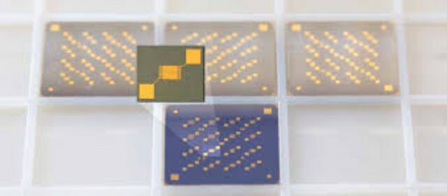
n-doped silicon wafer with 230 nm SiO2 gate-insulator, chips (diced)
About This Item
Productos recomendados
form
chips (diameter 200 mm)
chips (diced)
packaging
pack of 1 (wafer of 112 diced chips)
General description
Layer structure:
- Gate: n-doped silicon (doping at wafer surface: n~3x10¹⁷/ cm3)
- Gate oxide: 230 nm ± 10 nm SiO2 (thermal oxidation)
- Drain/source:none
- Protection: resist AR PC 5000/3.1 (soluble in AZ-Thinner or acetone)
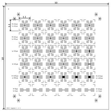
- Layout: bare oxide but diced
- Chip size: 15 x 15 mm2
- No. of chips: 112 per wafer
Application
These back-gated organic filed-effect transistor (OFET) substrates were fabricated inside the cleanroom, and source and drain electrodes can be deposited either prior or after the deposition of an organic semiconductor material, giving versatility for the choice of source/drain materials and satisfy different preferred device architectures.
When an organic semiconductor layer is deposited on such a substrate, the bulk Si acts as gate electrode and controls the channel current between the post-deposited source and drain electrodes on the top. A suitably doped Si-SiO2 interface in CMOS quality guarantees a reproducible gate contact.
Packaging
Preparation Note
To guarantee a complete cleaning of the wafer / chip surface from resist residuals, please rinse by acetone and then dry the material immediately by nitrogen (compressed air).
Recommendation for material characterization:
If gate currents appear during the characterization of the field effect transistors, considerable variations could occur at the extraction of the carrier mobility. Therefore it is necessary to check the leakage currents over the reverse side (over the chip edges) of the OFET-substrates.
Storage and Stability
Legal Information
Certificados de análisis (COA)
Busque Certificados de análisis (COA) introduciendo el número de lote del producto. Los números de lote se encuentran en la etiqueta del producto después de las palabras «Lot» o «Batch»
¿Ya tiene este producto?
Encuentre la documentación para los productos que ha comprado recientemente en la Biblioteca de documentos.
Artículos
Professor Tokito and Professor Takeda share their new materials, device architecture design principles, and performance optimization protocols for printed and solution-processed, low-cost, highly flexible, organic electronic devices.
Nuestro equipo de científicos tiene experiencia en todas las áreas de investigación: Ciencias de la vida, Ciencia de los materiales, Síntesis química, Cromatografía, Analítica y muchas otras.
Póngase en contacto con el Servicio técnico


