추천 제품
양식
chips (diced)
chips (each 15 x 15 mm2)
포장
pack of 1 (wafer of 60 diced chips)
저장 온도
15-25°C
유사한 제품을 찾으십니까? 방문 제품 비교 안내
일반 설명
Substrate: 150 mm wafer according to semiconductor standard (used for bottom-gate)
Layer structure:
4 x transistors L= 2.5 μm W= 10 mm
4 x transistors L= 5 μm W= 10 mm
4 x transistors L= 10 μm W= 10 mm
4 x transistors L= 20 μm W= 10 mm
Layer structure:
- Gate: n-doped silicon (doping at wafer surface: n~3x10¹⁷/ cm3)
- Gate oxide: 230 nm ± 10 nm SiO2 (thermal oxidation)
- Drain/source: 30 nm Au with 10 nm high work function adhesion layer (ITO), by lift-off technique
- Protection: resist AR PC 5000/3.1 (soluble in AZ-Thinner or acetone)
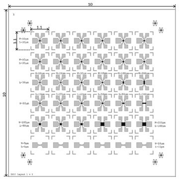
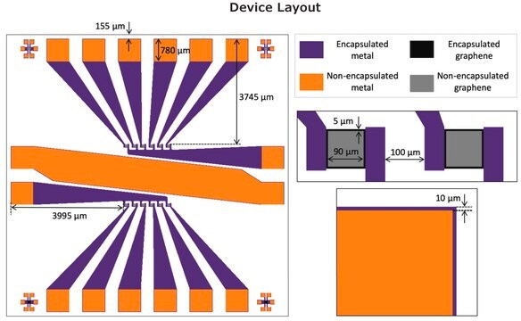
- Layout: see images
- Test chip size: 15 x 15 mm2
- No. of chips: 60 per wafer
- Contact pads: 0.5 x 0.5 mm2
- No. of transistors: 16 per chip
4 x transistors L= 2.5 μm W= 10 mm
4 x transistors L= 5 μm W= 10 mm
4 x transistors L= 10 μm W= 10 mm
4 x transistors L= 20 μm W= 10 mm
애플리케이션
Back-gated OFET Interdigitated Substrate (organic field-effect transistor) can be used in the fabrication of chemical sensors for potential usage in pH sensing and detection of immunoassays. It can also be used in the fabrication of biosensors by coating the sheets of the FET with a specific antibody for the detection of SARS-CoV-2. FET based biosensors can be potentially used in clinical diagnosis, point of care testing, and on-site detection.
포장
diced wafer on foil with air tight packaging
제조 메모
Recommendation for resist removal:
To guarantee a complete cleaning of the wafer / chip surface from resist residuals, please rinse by acetone and then dry the material immediately by nitrogen (compressed air).
Recommendation for material characterization:
If gate currents appear during the characterization of the field effect transistors, considerable variations could occur at the extraction of the carrier mobility. Therefore it is necessary to check the leakage currents over the reverse side (over the chip edges) of the OFET-substrates.
저장 및 안정성
Store the wafers at a cool and dark place and protect them against sun.
Resist layer was applied to prevent damage from scratches.
Expiration date is the recommended period for resist removal only. After resist removal, the substrate remains functional and does not expire.
Resist layer was applied to prevent damage from scratches.
Expiration date is the recommended period for resist removal only. After resist removal, the substrate remains functional and does not expire.
법적 정보
Product of Fraunhofer IPMS
가장 최신 버전 중 하나를 선택하세요:
The impact of biosensing in a pandemic outbreak: COVID-19
Morales-Narvaez E and Dincer C
Biosensors And Bioelectronics, 14(4), 112274-112274 (2020)
Polymer composite-based OFET sensor with improved sensitivity towards nitro based explosive vapors
Dudhe RS, et al.
Sensors and Actuators B, Chemical, 148(1), 158-165 (2010)
Rapid detection of COVID-19 causative virus (SARS-CoV-2) in human nasopharyngeal swab specimens using field-effect transistor-based biosensor
Seo G, et al.
ACS Nano, 14(4), 5135-5142 (2020)
Random CNT network and regioregular poly (3-hexylthiophen) FETs for pH sensing applications: A comparison
Munzer AM, et al.
Biochim. Biophys. Acta Gen. Subj., 1830(9), 4353-4358 (2013)
문서
Professor Tokito and Professor Takeda share their new materials, device architecture design principles, and performance optimization protocols for printed and solution-processed, low-cost, highly flexible, organic electronic devices.
자사의 과학자팀은 생명 과학, 재료 과학, 화학 합성, 크로마토그래피, 분석 및 기타 많은 영역을 포함한 모든 과학 분야에 경험이 있습니다..
고객지원팀으로 연락바랍니다.


