
推荐产品


产品名称
单层石墨烯薄膜, 1 cm x 1 cm on quartz, avg. no. of layers, 1
形狀
film
特點
avg. no. of layers 1
電阻
600 Ω/sq
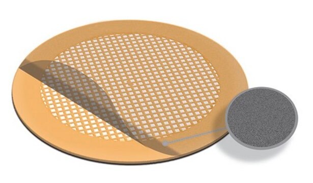
長度 × 寬度 × 厚度
1 cm × 1 cm × (theoretical) 0.345 nm, monolayer graphene film
1.25 cm × 1.25 cm × 525 μm, quartz substrate
正在寻找类似产品? 访问 产品对比指南
一般說明
Transfer Method: Clean transfer method
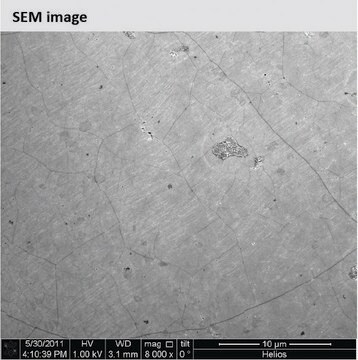
Quality Control: Optical Microscopy & Raman checked
Size: 1 cm x 1 cm
Appearance (Color): Transparent
Transparency: >97%
Appearance (Form): Film
Coverage: >95%
Number of graphene layers: 1
Thickness (theoretical): 0.345 nm
FET Electron Mobility on Al2O3: 2; 000 cm2/V·s
FET Electron Mobility on SiO2/Si (expected): 4; 000 cm2/V·s
Sheet Resistance: 600 Ohms/sq.
Grain size: Up to 10 μm
Substrate Quartz
Size: 1.25 cm x 1.25 cm
Flatness: bow: 20μm; warp: 30μm
Roughness:6 angstroms (on the polished side)
Surface: Double side polished
應用


訊號詞
Danger
危險分類
Carc. 1B - Eye Irrit. 2 - STOT RE 1 Inhalation - STOT SE 3
標靶器官
Lungs, Respiratory system
儲存類別代碼
6.1D - Non-combustible acute toxic Cat.3 / toxic hazardous materials or hazardous materials causing chronic effects
水污染物質分類(WGK)
WGK 3
閃點(°F)
Not applicable
閃點(°C)
Not applicable
商品
Graphene is a one-atomic-layer thick two-dimensional material made of carbon atoms arranged in a honeycomb structure. Its fascinating electrical, optical, and mechanical properties ignited enormous interdisciplinary interest from the physics, chemistry, and materials science fields.
Graphene has emerged as the new wonder material. Being only one atom thick and composed of carbon atoms arranged in a hexagonal honeycomb lattice structure, the interest in this material has exploded exponentially since 2004 when it was first isolated and identified using a very simple method.
A transparent conductive electrode (TCE) is an essential component of various optoelectronic devices such as solar cells, liquid-crystal displays (LCD), light-emitting diodes (LED), and touch screens.
我们的科学家团队拥有各种研究领域经验,包括生命科学、材料科学、化学合成、色谱、分析及许多其他领域.
联系技术服务部门