
推荐产品


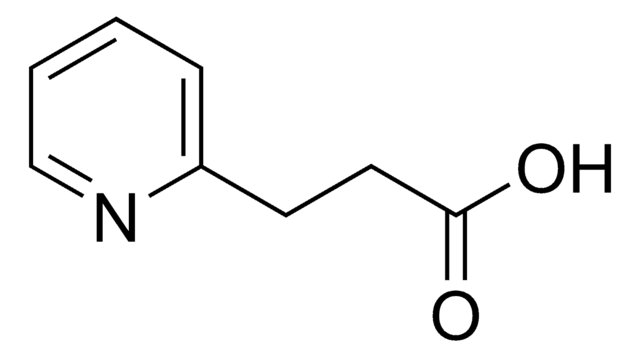
![2-[2-(Dicyclohexylphosphino)phenyl]-N-methylindole 97%](/deepweb/assets/sigmaaldrich/product/structures/224/910/4302f379-b335-4352-9f7d-67b84861582f/640/4302f379-b335-4352-9f7d-67b84861582f.png)

化驗
99.999% trace metals basis
形狀
solid
反應適用性
core: silicon
直徑× 厚度
2.00 in. × 0.25 in.
bp
2355 °C (lit.)
mp
1410 °C (lit.)
密度
2.33 g/mL at 25 °C (lit.)
SMILES 字串
[Si]
InChI
1S/Si
InChI 密鑰
XUIMIQQOPSSXEZ-UHFFFAOYSA-N
正在寻找类似产品? 访问 产品对比指南
應用
Sputtering is a process whereby atoms are ejected from a solid target material due to bombardment of the target by energetic particles. The extreme miniaturization of components in the semiconductor and electronics industry requires high purity sputtering targets for thin film deposition
儲存類別代碼
13 - Non Combustible Solids
水污染物質分類(WGK)
WGK 3
閃點(°F)
Not applicable
閃點(°C)
Not applicable
Kostantinidis, S.; et al.
The European Physical Journal - Applied Physics, 56, 24002/1-24002/1 (2011)
Helmersson; U.; et al.
Thin Solid Films, 513, 1-1 (2006)
Hyunhui Kim et al.
Journal of nanoscience and nanotechnology, 13(5), 3559-3563 (2013-07-19)
Silicon sheets were fabricated by a new fabricating method, spin casting with various rotation speeds of the graphite mold. The microstructure of spin-cast silicon sheets were investigated using an electron probe microanalyzer (EPMA) and scanning electron microscope/electron backscatter diffraction/orientation image
Si-nanowire-array-based NOT-logic circuits constructed on plastic substrates using top-down methods.
Youngin Jeon et al.
Journal of nanoscience and nanotechnology, 13(5), 3350-3353 (2013-07-19)
Si-nanowire (NW)-array-based NOT-logic circuits were constructed on plastic substrates. The Si-NW arrays were fabricated on a Si wafer through top-down methods, including conventional photolithography and crystallographic wet etching, and transferred onto the plastic substrates. Two field-effect transistors were fabricated on
Jae Cheol Shin et al.
Journal of nanoscience and nanotechnology, 13(5), 3511-3514 (2013-07-19)
We have characterized the structural properties of the ternary In(x)Ga(1-x)As nanowires (NWs) grown on silicon (Si) substrates using metalorganic chemical vapor deposition (MOCVD). Au catalyzed vapor-liquid-solid (VLS) mode was used for the NW growth. The density of the In(x)Ga(1-x)As NW
商品
Nanocomposite Coatings with Tunable Properties Prepared by Atomic Layer Deposition
Spin-based electronic (spintronic) devices offer significant improvement to the limits of conventional charge-based memory and logic devices which suffer from high power usage, leakage current, performance saturation, and device complexity.
The properties of many devices are limited by the intrinsic properties of the materials that compose them.
我们的科学家团队拥有各种研究领域经验,包括生命科学、材料科学、化学合成、色谱、分析及许多其他领域.
联系技术服务部门