FIPMS176
Back-gated OFET Substrate
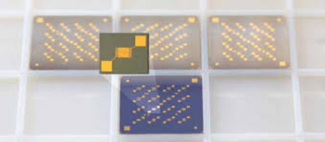
n-doped silicon wafer with 230 nm SiO2 gate-insulator, chips (diced)
About This Item
Prodotti consigliati
Forma fisica
chips (diameter 200 mm)
chips (diced)
Confezionamento
pack of 1 (wafer of 112 diced chips)
Descrizione generale
Layer structure:
- Gate: n-doped silicon (doping at wafer surface: n~3x10¹⁷/ cm3)
- Gate oxide: 230 nm ± 10 nm SiO2 (thermal oxidation)
- Drain/source:none
- Protection: resist AR PC 5000/3.1 (soluble in AZ-Thinner or acetone)
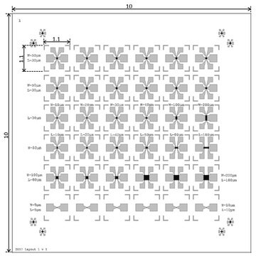
- Layout: bare oxide but diced
- Chip size: 15 x 15 mm2
- No. of chips: 112 per wafer
Applicazioni
These back-gated organic filed-effect transistor (OFET) substrates were fabricated inside the cleanroom, and source and drain electrodes can be deposited either prior or after the deposition of an organic semiconductor material, giving versatility for the choice of source/drain materials and satisfy different preferred device architectures.
When an organic semiconductor layer is deposited on such a substrate, the bulk Si acts as gate electrode and controls the channel current between the post-deposited source and drain electrodes on the top. A suitably doped Si-SiO2 interface in CMOS quality guarantees a reproducible gate contact.
Confezionamento
Nota sulla preparazione
To guarantee a complete cleaning of the wafer / chip surface from resist residuals, please rinse by acetone and then dry the material immediately by nitrogen (compressed air).
Recommendation for material characterization:
If gate currents appear during the characterization of the field effect transistors, considerable variations could occur at the extraction of the carrier mobility. Therefore it is necessary to check the leakage currents over the reverse side (over the chip edges) of the OFET-substrates.
Stoccaggio e stabilità
Note legali
Certificati d'analisi (COA)
Cerca il Certificati d'analisi (COA) digitando il numero di lotto/batch corrispondente. I numeri di lotto o di batch sono stampati sull'etichetta dei prodotti dopo la parola ‘Lotto’ o ‘Batch’.
Possiedi già questo prodotto?
I documenti relativi ai prodotti acquistati recentemente sono disponibili nell’Archivio dei documenti.
Articoli
Professor Tokito and Professor Takeda share their new materials, device architecture design principles, and performance optimization protocols for printed and solution-processed, low-cost, highly flexible, organic electronic devices.
Il team dei nostri ricercatori vanta grande esperienza in tutte le aree della ricerca quali Life Science, scienza dei materiali, sintesi chimica, cromatografia, discipline analitiche, ecc..
Contatta l'Assistenza Tecnica.


