
FIPMS148
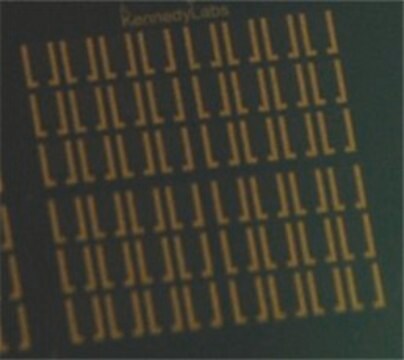
Back-gated OFET Interdigitated Substrate
Au source/drain, 230 nm SiO2 gate-insulator, varied W/L from 500 to 4000, 16 transistors per chip, chips (diced)
About This Item
Productos recomendados


Formulario
chips (diced)
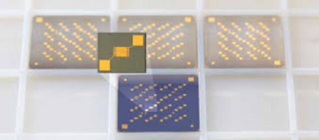
chips (each 15 x 15 mm2)
envase
pack of 1 (wafer of 60 diced chips)
temp. de almacenamiento
15-25°C
¿Está buscando productos similares? Visita Guía de comparación de productos
Descripción general
Layer structure:
- Gate: n-doped silicon (doping at wafer surface: n~3x10¹⁷/ cm3)
- Gate oxide: 230 nm ± 10 nm SiO2 (thermal oxidation)
- Drain/source: 30 nm Au with 10 nm high work function adhesion layer (ITO), by lift-off technique
- Protection: resist AR PC 5000/3.1 (soluble in AZ-Thinner or acetone)
- Layout: see images
- Test chip size: 15 x 15 mm2
- No. of chips: 60 per wafer
- Contact pads: 0.5 x 0.5 mm2
- No. of transistors: 16 per chip
4 x transistors L= 2.5 μm W= 10 mm
4 x transistors L= 5 μm W= 10 mm
4 x transistors L= 10 μm W= 10 mm
4 x transistors L= 20 μm W= 10 mm
Aplicación
Envase
Nota de preparación
To guarantee a complete cleaning of the wafer / chip surface from resist residuals, please rinse by acetone and then dry the material immediately by nitrogen (compressed air).
Recommendation for material characterization:
If gate currents appear during the characterization of the field effect transistors, considerable variations could occur at the extraction of the carrier mobility. Therefore it is necessary to check the leakage currents over the reverse side (over the chip edges) of the OFET-substrates.
Almacenamiento y estabilidad
Resist layer was applied to prevent damage from scratches.
Expiration date is the recommended period for resist removal only. After resist removal, the substrate remains functional and does not expire.
Información legal
Elija entre una de las versiones más recientes:
Certificados de análisis (COA)
It looks like we've run into a problem, but you can still download Certificates of Analysis from our Documentos section.
Si necesita más asistencia, póngase en contacto con Atención al cliente
¿Ya tiene este producto?
Encuentre la documentación para los productos que ha comprado recientemente en la Biblioteca de documentos.
Artículos
Professor Tokito and Professor Takeda share their new materials, device architecture design principles, and performance optimization protocols for printed and solution-processed, low-cost, highly flexible, organic electronic devices.
Global Trade Item Number
| Número de referencia del producto (SKU) | GTIN |
|---|---|
| FIPMS148-1PAK |
Nuestro equipo de científicos tiene experiencia en todas las áreas de investigación: Ciencias de la vida, Ciencia de los materiales, Síntesis química, Cromatografía, Analítica y muchas otras.
Póngase en contacto con el Servicio técnico