
推薦產品


產品名稱
R2R Monolayer large grain CVD graphene on silicon wafer, 6 in diameter, avg. no. of layers, 1
品質等級
描述
Growth method: roll-to-roll CVD
Wafer: SiO2 (300nm) Si
Number of layer: Monolayer
Raman intensity 2D/G: ≥1.5
特點
avg. no. of layers 1
薄層電阻
280 Ω/sq ±10%
尺寸
110 μm × 110 μm ± 10%, grain size
表面覆盖率
surface coverage >98%
透射率
>97%
半導體屬性
(mobility>3000 cm2/V·s) (Hall effect measurements)
SMILES 字串
NC.NC.NC.NC.NC.NC.NC.NC.NC
InChI
1S/9CH5N/c9*1-2/h9*2H2,1H3
InChI 密鑰
DXIFQVRACSPGSU-UHFFFAOYSA-N
尋找類似的產品? 前往 產品比較指南
一般說明
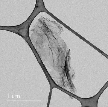
Roll-to-roll, high-quality, monolayer CVD graphene with large grain size (~110μm^2) on 6 inch silicon wafer.
應用
Our Roll-to-Roll CVD graphene products are true monolayer high quality graphene, fabricated inside a Cleanroom, heavily monitored and QC to assure high reproducibility.
The roll-to-roll process allows continuous, large scale graphene production.
This large grain size graphene product on silicon wafer is ready to use, helps you minimize process time, and increase success rate. This product with low sheet resistance would enable unmatched reproducibility and allow high performance for CVD graphene based FET, CVD graphene based sensors, and heterostructure based micro/nano electronics.
Application examples:
- Ultrafast Transistor
- Optical devices
- Bio/Gas Sensor
- Transparent Electrode
- Flexible Display
- Smart Coating
- Thermal management
注意
Be cautious not to drop
Keep away from contamination, heat, dust and flame etc.
Keep away from contamination, heat, dust and flame etc.
儲存和穩定性
Avoid direct sun light, avoid high temperature, avoid high humidity, and avoid dust.
法律資訊
Product of LG Electronics, R&D use only
儲存類別代碼
11 - Combustible Solids
水污染物質分類(WGK)
WGK 3
Integrating graphene into semiconductor fabrication lines.
Daniel Neumaier et al.
Nature materials, 18(6), 525-529 (2019-05-23)
Bing Deng et al.
Advanced materials (Deerfield Beach, Fla.), 31(9), e1800996-e1800996 (2018-10-03)
Chemical vapor deposition (CVD) is considered to be an efficient method for fabricating large-area and high-quality graphene films due to its excellent controllability and scalability. Great efforts have been made to control the growth of graphene to achieve large domain
我們的科學家團隊在所有研究領域都有豐富的經驗,包括生命科學、材料科學、化學合成、色譜、分析等.
聯絡技術服務