
推薦產品


產品名稱
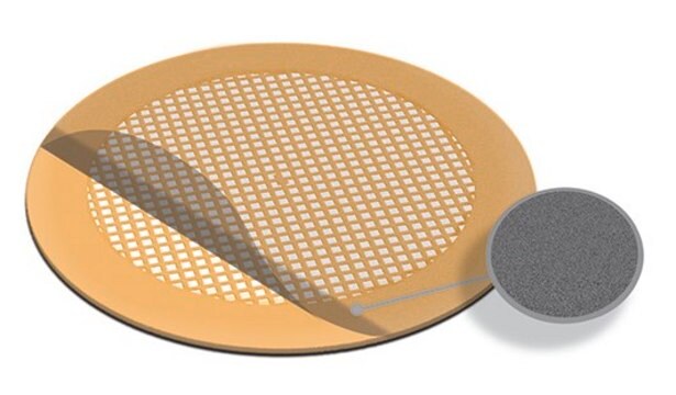
单层石墨烯薄膜, 1 cm x 1 cm on quartz, avg. no. of layers, 1
品質等級
形狀
film
特點
avg. no. of layers 1
電阻
600 Ω/sq
長度 × 寬度 × 厚度
1 cm × 1 cm × (theoretical) 0.345 nm, monolayer graphene film
1.25 cm × 1.25 cm × 525 μm, quartz substrate
尋找類似的產品? 前往 產品比較指南
一般說明
Transfer Method: Clean transfer method
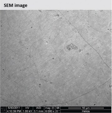
Quality Control: Optical Microscopy & Raman checked
Size: 1 cm x 1 cm
Appearance (Color): Transparent
Transparency: >97%
Appearance (Form): Film
Coverage: >95%
Number of graphene layers: 1
Thickness (theoretical): 0.345 nm
FET Electron Mobility on Al2O3: 2; 000 cm2/V·s
FET Electron Mobility on SiO2/Si (expected): 4; 000 cm2/V·s
Sheet Resistance: 600 Ohms/sq.
Grain size: Up to 10 μm
Substrate Quartz
Size: 1.25 cm x 1.25 cm
Flatness: bow: 20μm; warp: 30μm
Roughness:6 angstroms (on the polished side)
Surface: Double side polished
應用


訊號詞
Danger
危險分類
Carc. 1B - Eye Irrit. 2 - STOT RE 1 Inhalation - STOT SE 3
標靶器官
Lungs, Respiratory system
儲存類別代碼
6.1D - Non-combustible acute toxic Cat.3 / toxic hazardous materials or hazardous materials causing chronic effects
水污染物質分類(WGK)
WGK 3
閃點(°F)
Not applicable
閃點(°C)
Not applicable
文章
Professor Gogotsi and Dr. Shuck introduce MXenes: a promising family of two-dimensional materials with a unique combination of high conductivity, hydrophilicity, and extensive tunability.
Advanced technologies for energy conversion and storage are widely sought after for their potential to improve consumer and electronic device performance as well as for the prospect of reducing the societal and environmental impact of energy generation.
Graphene has emerged as the new wonder material. Being only one atom thick and composed of carbon atoms arranged in a hexagonal honeycomb lattice structure, the interest in this material has exploded exponentially since 2004 when it was first isolated and identified using a very simple method.
Global Trade Item Number
| 庫存單位 | GTIN |
|---|---|
| 773719-4EA | 4061832930930 |
我們的科學家團隊在所有研究領域都有豐富的經驗,包括生命科學、材料科學、化學合成、色譜、分析等.
聯絡技術服務