900527
Doped graphene
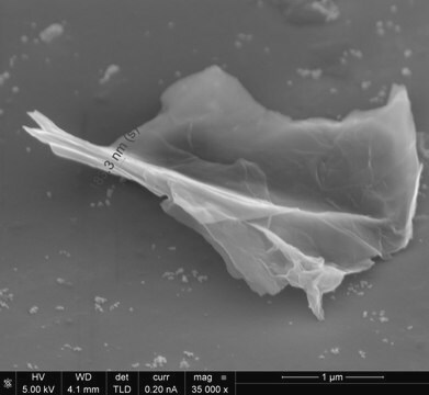
nitrogen-doped, avg. no. of layers, 1 ‑ 5
Synonym(s):
N-Doped graphene, NDG, NG
Sign Into View Organizational & Contract Pricing
All Photos(1)
About This Item
UNSPSC Code:
12141908
NACRES:
NA.23
Recommended Products
Product Name
Nitrogen-doped graphene, avg. no. of layers, 1 ‑ 5
Assay
≥95%
Quality Level
form
powder
feature
avg. no. of layers 1 ‑ 5
composition
Carbon, 85-95%
Nitrogen, 2.0-4.0%
Oxygen, <7.5%
surface area
>500 m2/g , BET
Looking for similar products? Visit Product Comparison Guide
Related Categories
General description
- Typical thickness: 1-5 layers.
- Typical size : 0.5-5 μm.
Application
- Electro catalyst.
- Field-effect transistors.
- Sensors.
- Lithium ion batteries.
- Supercapacitors.
Storage Class Code
11 - Combustible Solids
WGK
WGK 3
Flash Point(F)
Not applicable
Flash Point(C)
Not applicable
Choose from one of the most recent versions:
Certificates of Analysis (COA)
Lot/Batch Number
Don't see the Right Version?
If you require a particular version, you can look up a specific certificate by the Lot or Batch number.
Already Own This Product?
Find documentation for the products that you have recently purchased in the Document Library.
Andrea Zitolo et al.
Nature materials, 14(9), 937-942 (2015-08-11)
While platinum has hitherto been the element of choice for catalysing oxygen electroreduction in acidic polymer fuel cells, tremendous progress has been reported for pyrolysed Fe-N-C materials. However, the structure of their active sites has remained elusive, delaying further advance.
Review on recent progress in nitrogen-doped graphene: synthesis, characterization, and its potential applications.
Wang, et al.
ACS Catalysis, 2(5), 781-794 (2012)
Liangti Qu et al.
ACS nano, 4(3), 1321-1326 (2010-02-17)
Nitrogen-doped graphene (N-graphene) was synthesized by chemical vapor deposition of methane in the presence of ammonia. The resultant N-graphene was demonstrated to act as a metal-free electrode with a much better electrocatalytic activity, long-term operation stability, and tolerance to crossover
Mohi Uddin Jewel et al.
Molecules (Basel, Switzerland), 25(5) (2020-03-04)
Fully inkjet-printed device fabrication is a crucial goal to enable large-area printed electronics. The limited number of two-dimensional (2D) material inks, the bottom-gated structures, and the low current on/off ratio of thin-film transistors (TFTs) has impeded the practical applications of
Our team of scientists has experience in all areas of research including Life Science, Material Science, Chemical Synthesis, Chromatography, Analytical and many others.
Contact Technical Service