
推荐产品


形狀
film
特點
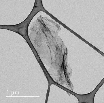
avg. no. of layers 1
電阻
600 Ω/sq
長度 × 寬度 × 厚度
1 cm × 1 cm × (theoretical) 0.345 nm, Monolayer graphene film
1.5 cm × 1.5 cm × 25 μm, copper foil substrate
正在寻找类似产品? 访问 产品对比指南
一般說明
Growth Method: CVD synthesis
Transfer Method: Clean transfer method
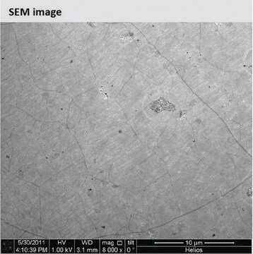
Quality Control: Optical Microscopy & Raman checked
Size: 1 cm x 1 cm
Appearance (Color): Transparent
Transparency: >97%
Appearance (Form): Film
Coverage: >95%
Number of graphene layers: 1
Thickness (theoretical): 0.345 nm
FET Electron Mobility on Al2O3: 2; 000 cm2/V·s
FET Electron Mobility on SiO2/Si (expected): 4; 000 cm2/V·s
Sheet Resistance: 600 Ohms/sq.
Grain size: Up to 10 μm
Substrate Copper Foil
Thickness: 25μm
Both sides: Graphene/Cu/Graphene
Packaging - 4 units/pack

訊號詞
Warning
危險聲明
危險分類
Eye Irrit. 2 - STOT SE 3
標靶器官
Respiratory system
儲存類別代碼
13 - Non Combustible Solids
水污染物質分類(WGK)
WGK 3
閃點(°F)
Not applicable
閃點(°C)
Not applicable
其他客户在看
商品
Developed in the last several years, fluorescence quenching microscopy (FQM) has enabled rapid, inexpensive, and high-fidelity visualization of two-dimensional (2D) materials such as graphene-based sheets and MoS2.
Professor Gogotsi and Dr. Shuck introduce MXenes: a promising family of two-dimensional materials with a unique combination of high conductivity, hydrophilicity, and extensive tunability.
Advanced technologies for energy conversion and storage are widely sought after for their potential to improve consumer and electronic device performance as well as for the prospect of reducing the societal and environmental impact of energy generation.
我们的科学家团队拥有各种研究领域经验,包括生命科学、材料科学、化学合成、色谱、分析及许多其他领域.
联系技术服务部门