FIPMS223
Back-gated OFET Interdigitated Substrate
Au source/drain, 90 nm SiO2 gate-insulator, varied W/L from 500 to 4000, 16 transistors per chip, chips (diced)
About This Item
Recommended Products
form
chips (diced)
packaging
pack of 1 (wafer of 60 diced chips)
storage temp.
15-25°C
Looking for similar products? Visit Product Comparison Guide
General description
Layer structure:
- Gate: n-doped silicon (doping at wafer surface: n~3x10¹⁷/ cm3)
- Gate oxide: 90 nm ± 10 nm SiO2 (thermal oxidation)
- Drain/source: 30 nm Au with 10 nm high work function adhesion layer (ITO), by lift-off technique
- Protection: resist AR PC 5000/3.1 (soluble in AZ-Thinner or acetone)
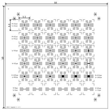
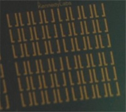
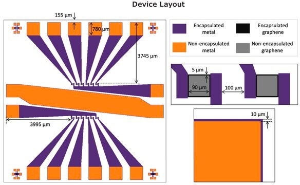
- Layout: see images
- Test chip size: 15 x 15 mm2
- No. of chips: 60 per wafer
- Contact pads: 0.5 x 0.5 mm2
- No. of transistors: 16 per chip
4 x transistors L= 2.5 μm W= 10 mm
4 x transistors L= 5 μm W= 10 mm
4 x transistors L= 10 μm W= 10 mm
4 x transistors L= 20 μm W= 10 mm
Application
Packaging
Preparation Note
To guarantee a complete cleaning of the wafer / chip surface from resist residuals, please rinse by acetone and then dry the material immediately by nitrogen (compressed air).
Recommendation for material characterization:
If gate currents appear during the characterization of the field effect transistors, considerable variations could occur at the extraction of the carrier mobility. Therefore it is necessary to check the leakage currents over the reverse side (over the chip edges) of the OFET-substrates.
Storage and Stability
Resist layer was applied to prevent damage from scratches.
Expiration date is the recommended period for resist removal only. After resist removal, the substrate remains functional and does not expire.
Legal Information
Choose from one of the most recent versions:
Certificates of Analysis (COA)
Sorry, we don't have COAs for this product available online at this time.
If you need assistance, please contact Customer Support.
Already Own This Product?
Find documentation for the products that you have recently purchased in the Document Library.
Articles
Professor Tokito and Professor Takeda share their new materials, device architecture design principles, and performance optimization protocols for printed and solution-processed, low-cost, highly flexible, organic electronic devices.
Our team of scientists has experience in all areas of research including Life Science, Material Science, Chemical Synthesis, Chromatography, Analytical and many others.
Contact Technical Service