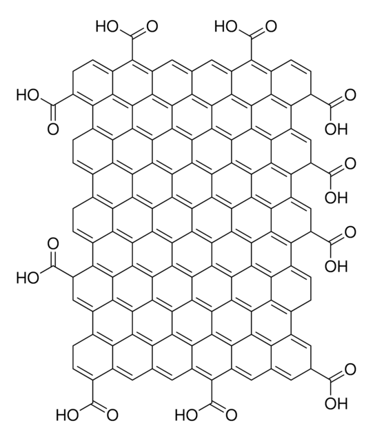
900443
Monolayer graphene film
1 cm x 1 cm on copper foil, with PMMA coating, avg. no. of layers, 1
Synonym(s):
PMMA/Graphene/Cu
About This Item
Quality Level
form
film
quality
Film coverage: >98% (optical)
Monolayer coverage: ≥92% (optical)
Raman analysis-monolayer
feature
avg. no. of layers 1
impurities
<2%
Looking for similar products? Visit Product Comparison Guide
Related Categories
General description
This product is provided with a PMMA coating on top of the graphene in order to ease the transfer process and to avoid contamination. It′s a high quality product with great homogeneity.
Graphene Film:
- Growth method: CVD synthesis.
- Appearance (color): Transparent.
- Transparency: >97%.
- Coverage: >98%.
- Number of graphene layers: 1.
- Thickness (theoretical): 0.345 nm.
- FET electron mobility on Al2O3: 2000 cm2/Vs.
- FET electron mobility on SiO2/Si: 4000 cm2/Vs.
- Sheet resistance on SiO2/Si: 450±40 Ω/sq (1cm x1cm).
- Grain size: Up to 10 μm.
Substrate Cu Foil:
- Thickness: 18 μm.
- Pre-treated for easier bottom layer removal. Monolayer graphene on the back side of copper is partially removed, but not completely. Therefore, an additional treatment like RIE is needed before transfer to eliminate the bottom layer totally.
PMMA Coating:
- Spin coated for high homogeneity.
- Molecular weight: 495k.
- Thickness: <100 nm.
- PMMA model: 495k, A2.
Application
- Flexible batteries.
- Electronics.
- Aerospace industry.
- MEMS and NEMS.
- Micro actuators.
- Conductive coatings.
Storage Class Code
13 - Non Combustible Solids
WGK
WGK 2
Flash Point(F)
Not applicable
Flash Point(C)
Not applicable
Certificates of Analysis (COA)
Search for Certificates of Analysis (COA) by entering the products Lot/Batch Number. Lot and Batch Numbers can be found on a product’s label following the words ‘Lot’ or ‘Batch’.
Already Own This Product?
Find documentation for the products that you have recently purchased in the Document Library.
Customers Also Viewed
Articles
Professor Ebrahimi and Professor Robinson (Pennsylvania State University, USA) summarize recent advances in the synthesis of these 2D materials, resulting material properties, and related applications in biosensing of neurotransmitters, metabolites, proteins, nucleic acids, bacterial cells, and heavy metals.
Professor Gogotsi and Dr. Shuck introduce MXenes: a promising family of two-dimensional materials with a unique combination of high conductivity, hydrophilicity, and extensive tunability.
Recent Advances in Scalable Synthesis and Processing of Two-Dimensional Materials
Our team of scientists has experience in all areas of research including Life Science, Material Science, Chemical Synthesis, Chromatography, Analytical and many others.
Contact Technical Service
