773700
Graphene, monolayer film
1 cm x 1 cm on SiO2/Si substrate, avg. no. of layers, 1
Synonym(s):
Single Layer Graphene Sheet
About This Item
Recommended Products
Product Name
Monolayer graphene film, 1 cm x 1 cm on SiO2/Si substrate, avg. no. of layers, 1
Quality Level
form
film
feature
avg. no. of layers 1
resistance
600 Ω/sq
L × W × thickness
1 cm × 1 cm × (theoretical) 0.345 nm, monolayer graphene film
1 cm × 1 cm × 525 μm, SiO2/Si substrate
Looking for similar products? Visit Product Comparison Guide
Related Categories
General description
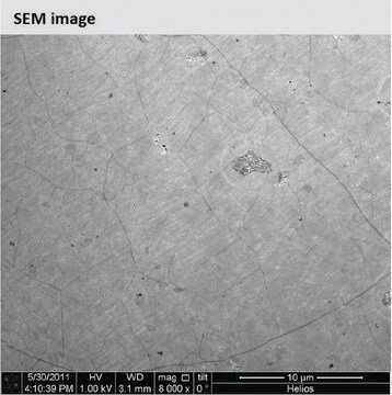
Growth Method: CVD synthesis
Transfer Method: Clean transfer method
Quality Control: Optical Microscopy & Raman checked
Size: 1 cm x 1 cm
Appearance (Color): Transparent
Transparency: >97%
Appearance (Form): Film
Coverage: >95%
Number of graphene layers: 1
Thickness (theoretical): 0.345 nm
FET Electron Mobility on Al2O3: 2; 000 cm2/V·s
FET Electron Mobility on SiO2/Si (expected): 4; 000 cm2/V·s
Sheet Resistance: 600 Ohms/sq.
Grain size: Up to 10 μm
Substrate
Size: 1.25 cm x 1.25 cm
Type/Dopant: P/B
Orientation: 100
Growth Method: CZ
Resistivity: 1-30 ohmcm
Thickness: 525 +/- 25μm
Front Surface: polished
Back Surface: etched
Coating: 300 nm thermal oxide on both wafer sides
Signal Word
Danger
Hazard Statements
Precautionary Statements
Hazard Classifications
Eye Irrit. 2 - STOT RE 1 Inhalation - STOT SE 3
Target Organs
Lungs, Respiratory system
Storage Class Code
6.1D - Non-combustible acute toxic Cat.3 / toxic hazardous materials or hazardous materials causing chronic effects
WGK
WGK 3
Flash Point(F)
Not applicable
Flash Point(C)
Not applicable
Choose from one of the most recent versions:
Already Own This Product?
Find documentation for the products that you have recently purchased in the Document Library.
Customers Also Viewed
Articles
Professor Gogotsi and Dr. Shuck introduce MXenes: a promising family of two-dimensional materials with a unique combination of high conductivity, hydrophilicity, and extensive tunability.
Graphene has emerged as the new wonder material. Being only one atom thick and composed of carbon atoms arranged in a hexagonal honeycomb lattice structure, the interest in this material has exploded exponentially since 2004 when it was first isolated and identified using a very simple method.
A transparent conductive electrode (TCE) is an essential component of various optoelectronic devices such as solar cells, liquid-crystal displays (LCD), light-emitting diodes (LED), and touch screens.
Our team of scientists has experience in all areas of research including Life Science, Material Science, Chemical Synthesis, Chromatography, Analytical and many others.
Contact Technical Service
