Dye-Sensitized and Perovskite Solar Cells: Interface Engineering by Atomic Layer Deposition
Valerio Zardetto1, Francesco Di Giacomo2, Thomas M. Brown2, Aldo Di Carlo2, Alessandra D’Epifanio3, Silvia Licoccia3, Erwin Kessels1, Mariadriana Creatore1
1Department of Applied Physics, Eindhoven University of Technology P.O. Box 513, 5600 MB Eindhoven, The Netherlands, 2Centre for Hybrid and Organic Solar Energy (CHOSE), Department of Electronic Engineering University of Rome “Tor Vergata,” via del Politecnico 1, 00133, Rome, Italy, 3Department of Chemical Science and Technologies, University of Rome “Tor Vergata,” Via della Ricerca Scientifica, 00133, Rome, Italy
Introduction
Since the demonstration of the first practical solar cell 60 years ago, research on novel materials, improved solar cell design and structure, and innovative manufacturing processes have all contributed to a continuous increase in the efficiency of photovoltaic (PV) devices.1 At a materials science level, fundamental studies primarily focus on the process of photocurrent generation, including charge carrier generation, charge transport and separation at the junction, and charge collection at the contacts. Equally important is the synthesis and development of highly absorbing thin active layers, as well as highly transparent and conductive contacts. The literature points out the importance of precisely engineering each interface of a PV structure at the nanoscale level in order to obtain higher power conversion efficiencies.2,3 For instance, in crystalline silicon (c-Si) PV devices, ultra-thin oxides applied to the front and back surface of the wafer significantly reduce charge surface recombination processes either through chemical- or fieldeffect passivation.2 Accurate control at the interface level is of the utmost importance for the most recent, low-cost PV technologies, such as organic photovoltaics (OPV), dye-sensitized solar cells (DSCs), and organometal halide perovskite solar cells, where nano- and mesostructured 3D interfaces are present. This additional understanding of the interface has contributed significantly to the recent increase in power conversion efficiency for both bulk heterojunction organic and polymer solar cells (BHJ-OPV) during the last years.3 Here, control of the photoactive BHJ layer is based on a nano-scale interpenetrating network of an electron acceptor and a donor polymer. This network rules the exciton dissociation and the charge transfer processes, while the interface between the BHJ and electrodes influences the charge extraction. The result is OPV performance approaching 10%,3,4 or even in excess of 10% in a tandem configuration.5
Atomic layer deposition (ALD) is a technique widely utilized in the PV field to meet the demand for sub-nm control over film properties and thickness.6 Ultra-thin Al2O3 layers have been successfully applied using ALD on the surface of crystalline silicon to form excellent passivation layers.7 In copper indium gallium (di)-selenide (CIGS) solar cells, where the control of the interface between the absorber and the n-type window layer is essential, cadmium-free ALD buffer layers such as (Zn,Mg)O and Zn(O,S) have been developed to improve the band alignment with the CIGS absorber.8 In this contribution, we first discuss the benefits of ALD when used for the fabrication of meso-structured DSCs and for hybrid organometal halide perovskite solar cells. In both architectures, the deposition of thin ALD metal oxides leads to an improvement in the device photo-voltage and current by suppressing selected interfacial charge recombination processes. In addition, we address the use of ALD for the deposition of Pt nanoparticles, which allows for efficient charge transfer at the interface between the liquid electrolyte and a highly transparent counter electrode (CE) in a flexible DSC.
Atomic Layer Deposition
ALD is a cyclic vapor phase deposition technique that enables the synthesis of thin films with atomic level control using sequential, selflimiting surface reactions (i.e., once all the active surface sites have reacted with the precursors, the reaction is completed). Figure 1 representss an ALD process based on the repetition of two half cycles. Self-limited reactions occur between the surface and the precursor (first half cycle) and then the reactant (second half cycle). Purge steps are required to guarantee the absence of a chemical vapor deposition (CVD) contribution since they avoid the direct contact between the precursor and reactant. Therefore, the film thickness increases linearly as a function of the number of ALD cycles.

Figure 1. Schematic representation of an ALD cycle.
The reactant in the second half cycle can be water vapor, for example, for oxides. In this case, the reaction is driven by the temperature of the surface/substrate (Thermal ALD). Thermal ALD provides superior uniformity over large areas and excellent conformability in structures with a high aspect ratio, such as porous and nanostructured films. Plasma-assisted ALD is an alternative approach in which the reactant dose is replaced with a plasma exposure step. Plasma-assisted ALD offers several advantages compared to thermal processes, especially at low temperatures. The high reactivity of the plasma species (ions, metastables, and radicals) allows for: (1) the tuning of the chemical composition of the layer; (2) the development of higher density films (e.g., through an accurate control of the ion energy and flux); and (3) processing at lower temperatures, even down to room temperature,9,10 making the process compatible with thermally sensitive substrates. One disadvantage of plasma-assisted ALD is reduced conformability, which particularly impacts the coating of complex 3D structures compared to other methods.11
Passivation Layers on Mesoscopic Structures
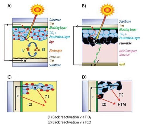
A conventional DSC (Figure 2A) is generally composed of a nanocrystalline TiO2 mesoporous film deposited on a transparent conductive oxide (TCO) coated glass or polymer substrate. Dye molecules are adsorbed on the large TiO2 surface area and act as light harvesters. A redox liquid electrolyte (e.g., I-/I3-) and a counter electrode (Pt/TCO/substrate) complete the architecture.12

Figure 2. Configuration of hybrid mesoscopic solar cells: A) dye-sensitized and B) perovskite solar cells. The application of passivation and blocking layers has the purpose of limiting the primary interfacial back reactions in C) dye-sensitized and D) perovskite solar cells.
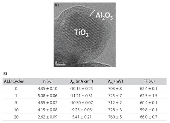
While the mesoporous structure is useful for efficient light harvesting, the huge internal surface area also increases recombination processes at the interface between the non-sensitized TiO2 matrix and the liquid electrolyte. Here back charge transfer reactions occur between the electrons and the oxidized species (I3-),13 as shown in Figure 2C. The application of an ultra-thin dielectric layer, generally a wide band gap metal oxide (Al2O3, HfO2, Ga2O3),14–16 to form a high recombination energy barrier (Figure 3A) is a well-known strategy for reducing this recombination mechanism. In Figure 3A, thermal ALD was used to deposit an Al2O3 layer on TiO2 nanoparticles (Prod. No. 791326)—precise control of the oxide film thickness is essential to enable a sufficient passivation without reducing electron injection efficiency via tunnelling from the dye molecules to the TiO2 conduction band.
The deposition of a single Al2O3 ALD cycle leads to the best results in terms of short circuit current (JSC) and open circuit voltage (VOC) and, consequently, in terms of power conversion efficiency (+17%) (Figure 3B). Increasing the Al2O3 thickness with the number of ALD cycles (over 5) reduces the short circuit current (JSC), although an increment of the VOC is also observed. The presence of the ultra-thin ALD layer influences the energy barrier height at the Al2O3/TiO2 and Al2O3/dye interfaces, thereby controlling the recombination and the electron charge transfer processes, respectively.17 A thicker Al2O3 layer is responsible for the reduction in tunnelling through the metal oxide and the suppression of the back reaction, therefore decreasing the JSC value.

Figure 3.A) High-resolution TEM of thermal ALD Al2O3 on a nanocrystalline TiO2 mesoporous film. B) Photovoltaic performance in terms of efficiency (η), short circuit current (JSC), open circuit voltage (VOC), and fill factor (FF) at 1 SUN of illumination for DSCs (active area of 0.25 cm2) as a function of the number of ALD cycles.
Recently, replacement of the liquid electrolyte with a hole transport material (HTM) and breakthroughs using organolead halide perovskite as absorbers (generally CH3NH3PbX3 with X=halogen) have led to the development of completely solid-state devices (Figure 2B) with efficiency values as high as 17.9%.18 Although the ambipolar transport behavior of the perovskite also allows the fabrication of planar architectures similar to thin film PV devices, the application of a mesostructured TiO2 scaffold has been found to lead to superior efficiency and stability.19 In this architecture, the parasitic back reactions at the interface between the mesoporous TiO2 film and the hole conductor stack perovskite/HTM are found to limit the VOC of the device. An ultra-thin (2 nm) conformal ALD TiO2 layer applied over the mesoscopic structure has been shown to also act as a passivation layer in high-efficiency perovskite solar cells.20
Blocking Layers on Transparent Conductive Oxides
A second recombination pathway in DSCs is at the interface between the TCO and the liquid electrolyte (Figure 2C), where the electrons can be captured by the oxidized species (I3-). In solid-state perovskite solar cellsthe interface TCO/hole conductor (both the perovskite and HTL layer) is characterized by a significant back transfer process affecting device performance (Figure 2D).20–23 The current state-of-the art approach to reducing this recombination mechanism is the introduction of a blocking layer (BL) in both architectures. This layer must be extremely compact to exhibit rectifying behavior. ALD techniques are ideally suited for the delivery of such ultra-thin layers compared to other methodologies such as spray pyrolysis, sputtering, electrodeposition, and sol-gel.22,23 For example, thermal ALD has been used already for the deposition of an ultra-thin (5–10 nm) TiO2 compact layer on FTO/glass substrate for use in a DSC device.24
Plasma-assisted ALD allows the deposition of higher quality films on planar surfaces in a temperature range compatible with lightweight plastic substrates, which are suitable for low-cost manufacturing methods such as continuous roll-to-roll.25 Plasma-assisted ALD processes have been adopted to deposit TiO2 and ultra-thin Al2O3 and SiO2 blocking layers at 150 °C on indium tin oxide (ITO)/PEN in DSC architecture.26 The presence of a compact BL affects the cell performance depending on the level of illumination. Under full illumination (1 SUN), only a small variation in the generated power is discernible; whereas, under low level illumination, substantial improvements (Al2O3: +26%; SiO2: +33%; and TiO2: +40%) have been observed, as summarized in Figure 4.

Figure 4. Normalized power of the DSCs using Al2O3 (four ALD cycles), SiO2 (six ALD cycles), and TiO2 (100 ALD cycles) blocking layers deposited by plasma-assisted ALD as compared to a reference cell (REF) without a blocking layer at different irradiations (1 SUN and indoor - 300 lux with CFL lamp).
Introduction of compact BLs is relevant for low light intensity conditions, where the photogenerated current is in the order of
μA∙cm-2 instead of mA∙cm-2. This increase in the performance could be a crucial step for the exploitation of flexible DSCs for indoor applications and for their integration in portable electronics. In contrast, for high levels of illumination the slight variation is ascribed to the minor impact of the back charge transfer process at the ITO/electrolyte interface with respect to the photo-charge collection mechanism, as already observed in the presence of another TCO, fluorine tin oxide (FTO) used in glass-based devices.27
The electron recombination at the TCO/perovskite and hole conductor interfaces also has been recognized as a significant loss factor for perovskite solid-state devices. In particular, the back charge transfer process between the ITO surface and the hole conductor is important as a recombination channel, when compared to the same process occurring at the interface of the ITO/electrolyte in plastic-based DSCs and the FTO/hole conductor interface in glass-based perovskite solar cells.26,28 The absence of the blocking layer on an ITO/PET substrate is so detrimental that it has led to extremely low VOC values (50 mV). The deposition of an 11 nm thick TiO2 layer significantly decreases recombination and enables the fabrication of a flexible device with an efficiency of 7.4% (Figure 5).

Figure 5.Photocurrent density–voltage curve for the mesoscopic perovskite solar cell with (and without) the TiO2 blocking layer.
Platinum Nanoparticles on ITO/PEN Substrates
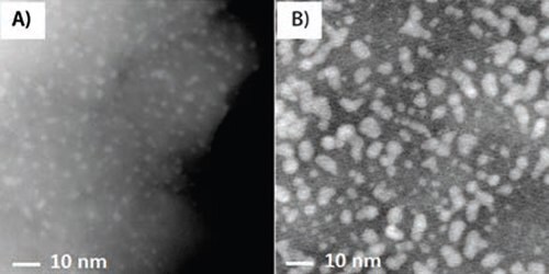
In the liquid-based DSC architecture, the interface between the platinum layer, generally composed of nanoparticles (NPs), and the electrolyte (Figure 2A) plays a key role in the charge transfer process for the reduction of the oxidized species I3 - to 3I-. Recently, low-temperature processing by plasma-assisted ALD has been successfully applied for the synthesis of platinum NPs (Prod. No. 685453),29 also on ITO/ PEN substrates30 (Figure 6). It has been found that the electro-catalytic properties of the counter-electrode are not only governed by the Pt loading but also by the NPs surface active area.30 At the same time, a limited Pt loading is required to guarantee a highly transparent electrode for efficient light harvesting in the case of back-illuminated flexible DSCs.

Figure 6.High-resolution TEM images of the platinum NPs prepared with 50 and 100 ALD cycles at 100 °C on ITO/PEN substrates.
Optimal cell power efficiency was achieved using 100 ALD cycles, corresponding to a Pt loading of 390 nm⋅cm-2 with an average particle size of 3 nm and a transparency of 95%. Furthermore, when compared to conventional methods (sputtering and electrodeposition) adopted in literature for ITO-polymer substrates, ALD-prepared NPs exhibit equivalent electro-catalytic activity properties but higher transparency (+10%), leading to an improved solar cell efficiency (+19%).30
Summary
Precise engineering and a high degree of control at the interfaces within a solar cell are vital for the improvement of its performance. The application of ALD to the latest generation of solar cells, such as dye-sensitized and perovskite, has been addressed here. Both thermal and plasmaassisted ALD approaches have been successfully adopted to fabricate dielectric and semiconductor ultra-thin films and metal nanoparticles on different substrates. ALD Al2O3 passivation layers on mesoporous structures and different compact blocking layers on TCOs suppress the charge recombination processes at complex interfaces within the device. Furthermore, control over the loading and size of Pt NPs on PEN/ITO substrates allows for a compromise between the charge transfer properties of the counter-electrode and its optical transparency for backside illuminated DSCs. All these applications demonstrate how ALD can be a successful approach for achieving nanoscale control in mesoscopic solar cells.
Acknowledgments
The colleagues of the Plasma & Materials Processing group (TU/e) are acknowledged for their contribution to the research. All ALD processes presented in this contribution were developed on FlexAl reactors in the cleanroom of NanoLab@TU/e. Fabrication procedures for DSCs and perovksite solar cells were developed in the cleanroom of CHOSE, University of Rome “Tor Vergata.” The synthesis of perovskite precursors was carried out at the Department of Chemical Science and Technologies, University of Rome “Tor Vergata.” Dr. M.A. Verheijen (TU/e) is acknowledged for electron microscopy images. The project ENERGY.2012.10.2.1 (NANOMATCELL, grant agreement no. 308997) is acknowledged for funding.
References
계속 읽으시려면 로그인하거나 계정을 생성하세요.
계정이 없으십니까?