The Savannah ALD System - An Excellent Tool for Atomic Layer Deposition
Dr. Douwe Monsma, Dr. Jill Becker
Material Matters 2006, 1.3, 5
Introduction
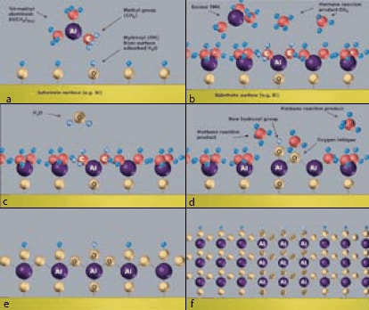
Atomic Layer Deposition (ALD) is a coating technology that allows perfectly conformal deposition onto complex 3D surfaces. The reason for this uniform coating lies in the saturative chemisorption of sequential cycles of precursor vapors. The process is illustrated in Figure 1. In Figure 1a, a silicon surface is terminated with hydroxyl groups (formed during contact with air). The wafer is inserted in an ALD reactor and a first precursor is introduced (here trimethyl aluminum, TMA, Figure 1a-b) using a fast pulse valve to a cylinder with liquid TMA. The precursor reacts with the surface layer, but not with itself, forming a single saturated monolayer. Subsequently, the TMA vapor and methane reaction products are pumped away and water vapor is introduced (Figure 1c-d). This forms a saturated monolayer of oxygen (Figure 1e) with a volatile reaction product of methane (again a saturated monolayer because the water molecules don’t react anymore after the water formed the hydroxyl (OH) passivated surface). The methane and water are pumped away and the cycle is repeated until the desired coating thickness is obtained (Figure 1f).

Figure 1a-f.Atomic Layer Deposition reaction cycle showing the formation of Al2O3 coating using trimethylaluminum (TMA) and water as precursors, and methane as volatile reaction product.
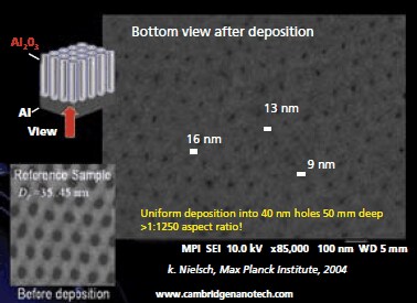
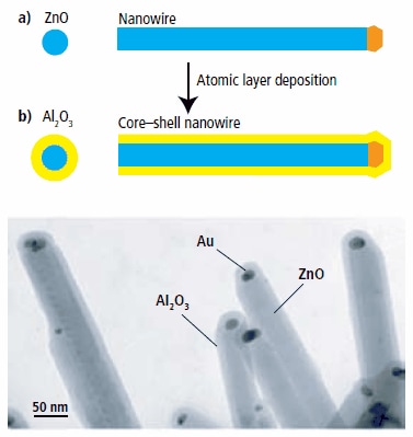
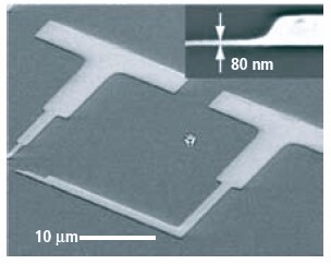
Since the films saturate to a monolayer with each precursor pulse, the coating will be equally thick inside small pores as on the surface of a substrate. This allows deposition inside photonic crystals, DRAM capacitor trenches, around suspended MEMS structures, around particles, etc. In fact, aspect ratios larger than 1:1000 can be routinely achieved using Cambridge NanoTech ALD systems; an example is shown in Figure 2 where a uniform coating is formed inside 50 nm dia, 50 micron deep pores in anodically etched aluminum oxide substrates and in Figure 3 where semiconductor nanowires have been coated conformally. For microelectronic applications, we have demonstrated lift-off of ALD coatings with nanometer resolution (Figure 4). Here we either used optical resist or e-beam resist to form patterned ALD coatings on silicon wafers. Dielectric and electronic properties have been tested using metal-insulator-metal capacitors. Dielectric constant and breakdown values for Al2O3, HfO2 and ZrO2 are listed in Table 1.

Figure 2. Conformal coatings inside anodic aluminum oxide substrates, with pores 50 microns deep conformally reduced in diameter from 40 nm to 20 nm, using Cambridge NanoTech ALD Systems.
The intrinsic deposition uniformity is an advantage for the ALD systems despite variability in process conditions. The deposition is relatively insensitive to variations of precursor flux over the substrate. In fact, usually overdosing is used to reach complete saturation, as well as to temperature variations. This makes ALD more repeatable and user friendly than chemical vapor deposition (CVD) or sputtering, where the thickness needs to be tracked constantly with a thickness monitor. Scaling is a further advantage of ALD. Batch reactors can be used where many substrates are stacked with small separations. All substrates can be coated at once with great uniformity. This in contrast to CVD where uniformity is compromised in batch systems, or sputtering where continuous line of sight with the sputter target is needed and batches are limited to only a couple of substrates, and very large targets and vacuum chambers are required.

Figure 3.Conformal coatings around semiconductor nanowires using Cambridge NanoTech ALD systems.2
To summarize the advantages of ALD:
- Thickness is determined simply by number of deposition cycles.
- Precursors are saturatively chemisorbed, which results in stoichiometric films with large area uniformity and 3D conformality.
- Relatively insensitive to dust (film grows underneath dust particles).
- Intrinsic deposition uniformity and small source size, implies easy scaling.
- Nanolaminates and mixed oxides are possible.
- Low temperature deposition is possible (RT-400C).
- Gentle deposition process for sensitive substrates.
Because of the active synthesis of ALD precursors by chemists, the number of materials that can be deposited is increasing rapidly, and with it the number of applications is mounting.
The Savannah ALD System
The Savannah ALD systems manufactured by Cambridge NanoTech Inc. have unique features not found in other ALD systems. The reactor volume is low, allowing fast cycle times and very little precursor consumption. This in turn permits the use of a smaller vacuum pump and small precursor cylinders, mounted underneath the reactor. The footprint of this ALD system is consequently the smallest on the market (typically only 20”320”). Despite its small size, substrates up to 200 mm can be deposited (Savannah 200 Model) with thickness uniformity and repeatability generally <+/-1% (Al2O3). With special lids, the height of the reactor can be modified to allow thick substrates and larger parts. Using a modular heated manifold, up to 6 precursors can be mounted, including solid, liquid, and gas precursors. All precursor heating is standard. Special 3-way ALD valves are employed that can be heated up to 200C, allowing a wide range of liquid and solid precursors to be used. The unique stop valve exposure mode allows deposition into narrow and deep pores, with aspect ratios larger than 1:1000 readily achieved.
The Savannah models have been outfitted in glovebox environments, allowing deposition onto air-sensitive substrates such as organic flat panel displays. In addition to the standard Savannah models, Cambridge NanoTech Inc. manufactures custom ALD systems for any substrate size. The Savannah models run in industrial and academic environments, both for specific R&D and general cleanroom use.

Figure 4. ALD Lift-off of various dielectric coatings using photoresist and ebeam resist with nanometer resolution.
Applications and Materials for ALD
In the field of micro- and nano-electronics, high-k dielectrics (Al2O3, HfO2, ZrO2, PrxAylOz, Ta2O5, La2O3), conductive gate electrodes (Ir, Pt, Ru, TiN) and metal interconnects (Cu, WN, TaN, Ru, Ir) have been applied. In particular, deposition onto semiconductors that do not form native oxides (such as SiO2) ALD has been proven essential.
Because of its ability to coat conformally around rough and particulate surfaces, catalytic coatings form an important field of application for ALD. For example, coatings inside filters, membranes, catalysts (thin economical Pt for automobile catalytic converters), and ion exchange coatings in fuel cells (Pt, Ir, Co, TiO2, V2O5).
Other important field of application are micro-electromechanical and nano-electromechanical systems (MEMS and NEMS). Here, suspended and 3D etched structures can easily be coated conformally using ALD. The same is true for biomedical devices, that often have complex shapes and can be coated with a variety of nitride ceramics.
In the field of optics, large improvements in uniformity of optical parameters and thickness can be obtained by using ALD. In addition, substrates don’t need to be rotated to be coated all over and batch processes can be applied to reduce cost. Several fields of optics benefit from ALD: nanophotonics, solar cells, integrated optics, lasers, variable dielectric constant nanolaminates, Fabry-Perot, Rugate, flip-flop optical filters, and anti-reflection coatings (Al2O3, ZnS, SnO2, Ta2O5, AlTiO, SnO2, ZnO). For photonic crystals and inverted opals, ALD is conveniently the only technique that can be used to internal coatings.
ALD is commercially used in the fabrication of magnetic read heads (for insulating layers, mainly Al2O3) as well as for flat panel displays. More recently, ALD has proven to create excellent humidity barriers for organic light emitting displays (OLEDs).
Several niche applications have been found as well, such as piezoelectric layers (ZnO, AlN, ZnS), transparent electrical conductors (ZnO:Al, ITO) and gas/pH sensors (SnO2, Ta2O5), wear, solid lubricant and corrosion inhibiting layers (Al2O3, ZrO2, WS2).
Besides many ceramics, ALD can now also deposit various metals, such as Ru, Pd, Ir, Pt, Rh, Co, Cu, Fe, and Ni, increasing the number of applications and advancing science by allowing precision coatings in places where no other technique has gone before.
References
Per continuare a leggere, autenticati o crea un account.
Non hai un Account?