TIPS Pentacene Dip Coating Procedure
Electronic Applications and Processes for TIPS Pentacene
With the discovery of organic semiconductors more than twenty years ago, researchers have constantly sought materials with superior performance and a lower cost of processing. Soluble semiconductors are a key part of developing low-cost circuits and flexible circuit design, enabling all-additive processing (single step for deposition and patterning) and eliminating the need for expensive subtractive steps involving traditional photolithography.
One of the best known and highest performing small-molecule organic semiconductors is TIPS pentacene (6,13-Bis[triisopropylsilylethynyl]pentacene). TIPS pentacene (Product No. 716006) is soluble in a wide range of solvents and does not require a thermal conversion after deposition. It is also stable in air, allowing easy handling without an inert atmosphere. With these benefits, it is critical to understand how to maximize the potential for TIPS pentacene and how it might be used in a wide variety of electronic applications and processes.
Preparation Instructions
Coating Solution – prepare a solution containing ~3.4 wt.% PVP and 1.1 wt.% poly(melamine-coformaldehyde) (Product No. 418560) in PGMEA solvent (Product No. 484431)
Semiconductor Solution – prepare a solution consisting of 2 wt.% TIPS-Pentacene (Product No. 716006) dissolved in a solvent blend consisting of 91% anisole (Product No. 296295) and 9% decane (Product No. 457116) by weight.
Semiconductor Dip Coating Procedure
As with all semiconductors, there are a number of critical parameters necessary to obtain the optimal performance of TIPS pentacene. Among other variables, these parameters include:
- complimentary choices in solvent
- deposition method
- drying method
- contact treatments
- dielectric material
- contact metal
With the right combination of parameters, TIPS pentacene has been demonstrated to achieve some of the highest mobility (up to 1.8 cm2/Vs)1 and performance results in the industry.
Fabrication
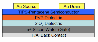
The TIPS pentacene semiconductor can be applied in a straightforward procedure using a dip coating method. Whereas specific procedures for specific devices will need to be developed by each scientist or engineer, this bulletin presents starting guidelines. For simplicity, a bottom gate thin film transistor (TFT) device is used as the example (Figure 1). With this dip process, TIPS pentacene should lead to excellent device performance, as well as consistent and repeatable results.

Figure 1.Cross-section of TIPS-Pentacene thin-film transistor
- Start with a heavily doped n-type silicon wafer (As) with 1,000 Å of thermal oxide on the front surface and coated with 100 Å titanium nitride and 5,000 Å aluminum on the back.
- Deposit a layer of poly(4-vinylphenol) (PVP, Product No. 436216) ~100 nm thick by spin coating the Coating Solution at 2,000 rpm.
- Place the sample on a hotplate for 2 minutes at 100 °C to evaporate the PGMEA followed by 30 minutes at 160 °C to effect the cure.
- Filter the Semiconductor Solution through a 0.2 mm PTFE filter (Product No. Z134171 or Z134201) before use.
- Use ~5 mL of Semiconductor Solution to fill the dip coating reservoir. This volume requires ~100 mg of semiconductor sample.
- Coat the semiconductor solution using a draw rate of 3–5 millimeters per minute using a vertical dip coating apparatus (e.g., NIMA D1L).
- After coating, allow the sample to dry at room temperature under atmospheric conditions. This dip coating method results in the formation of long crystals on the dielectric surface, typically oriented parallel to the dip axis (Figure 2).

Figure 2.TIPS-Pentacene film formed by dip coating
- Deposit gold source and drain electrodes (800–1,000 Å thick) via thermal evaporation through a shadow mask. Orient the source and drain contacts such that the direction of current flow is parallel to the dip coating axis, therefore, along the long axis of the crystals.
- In this example, the channel width and length were 1,000 μm and 100 μm, respectively. A cross-section of the device is shown in Figure 1.
Results
Calculations of hole mobility
The hole mobility (μ) can be calculated from the slope (m) of the plot of the square root of drain current versus VGS using the following equation:

The hole mobility (μ) can be calculated from the slope (m) of the plot of the square root of drain current versus VGS using the following equation:
C is the specific capacitance of the gate dielectric
W is the effective channel width
L is the channel length
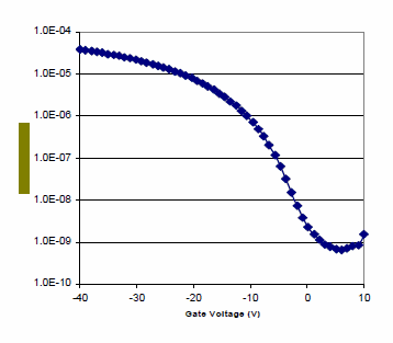
Measured mobility values are typically 0.3–0.4 cm2/Vs using this process, and on/off ratios are typically greater than 104. A typical ID-VGS plot is shown in Figure 3.

Figure 3.Typical ID-VGS transfer curve for a dip coated TIPSPentacene TFT
- Alternatively, the mobility can be calculated using the standard equation for drain current in a MOSFET:

The threshold voltage (VT) is estimated by extrapolating the linear portion of the square root of drain current versus VGS curve back to the x-axis.
If you have any additional questions, please contact Technical Service:
On the Web
Phone (US Only): 800-231-8327
References
TIPS-Pentacene is a product of 3M and this bulletin was developed in cooperation with the 3M Corporation.
To continue reading please sign in or create an account.
Don't Have An Account?